
Quantum Diamond Microscopy: Mapping Current Flow in the Next Generation of Semiconductors
For decades, diamond has been hailed as the "ultimate" semiconductor due to its extreme thermal and electrical properties, yet visualizing its internal mechanics has remained a significant challenge. By utilizing quantum nitrogen-vacancy (NV) centers embedded within the substrate, researchers have now successfully mapped current density in diamond transistors with unprecedented micrometer-scale resolution. This breakthrough, detailed in new research led by a collaborative team including Anuj Bathla and experts in hexagonal boron nitride (hBN) such as Kenji Watanabe and Takashi Taniguchi, offers a non-invasive window into the behavior of high-power electronics. The ability to "see" electricity moving through a solid diamond lattice could potentially accelerate the transition to more efficient energy grids, high-frequency communication systems, and robust electric vehicle (EV) powertrains.
The Diamond Frontier in Computing
As the limits of silicon-based electronics become increasingly apparent, the search for wide-bandgap materials has led scientists to diamond. Compared to conventional silicon, diamond possesses a significantly larger bandgap, exceptional carrier mobility, and the highest known thermal conductivity of any bulk material. These characteristics make it ideal for high-voltage stability and effective heat management, which are the primary bottlenecks in modern chip design. However, the development of diamond field-effect transistors (FETs) has been hampered by the difficulty of characterizing transport at buried interfaces. The research focuses on hydrogen-terminated diamond surfaces, where the interaction between the hydrogen atoms and the diamond lattice induces a two-dimensional hole gas (2DHG). This 2DHG acts as the conductive channel for the transistor, but until now, observing how current actually traverses this channel under a gate has been largely a matter of theoretical modeling rather than direct observation.
The Quantum Microscope: Seeing Through Solid Matter
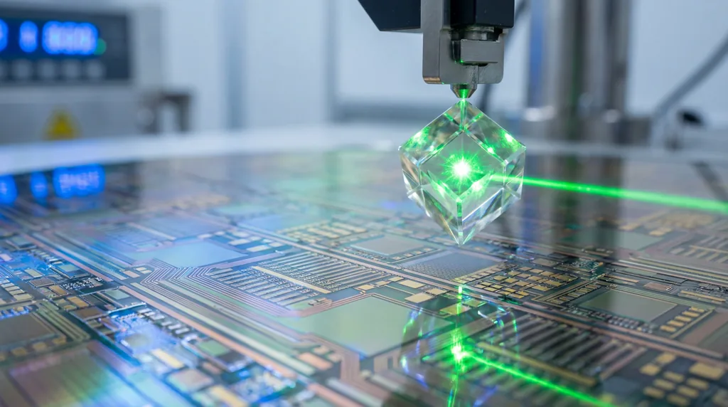
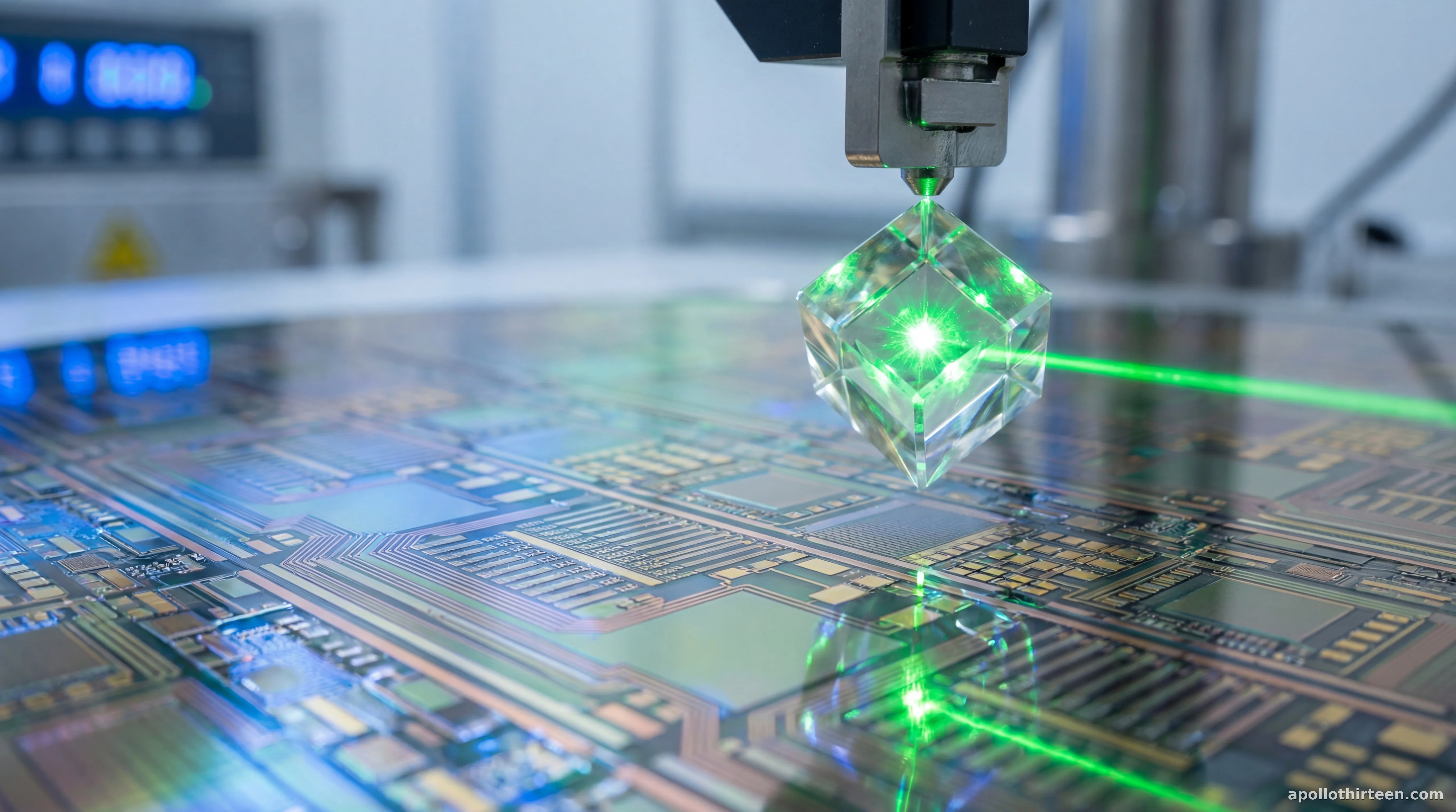
The core innovation of this study lies in the application of Widefield Quantum Diamond Microscopy (QDM). To achieve this, the researchers utilized Nitrogen-Vacancy (NV) centers—atomic-scale defects where a nitrogen atom and a vacuum site replace carbon atoms in the diamond lattice. These NV centers act as highly sensitive quantum sensors. Located approximately 1 micrometer below the diamond surface, an ensemble of these centers was used to perform non-invasive magnetic imaging of the device in operation. Because moving electrical charges generate magnetic fields, the NV centers can detect the magnetic signature of the current flowing through the 2DHG. By monitoring the spin states of these quantum defects via laser-induced fluorescence, the team was able to translate complex magnetic field data into vivid, two-dimensional maps of electricity without altering the device's function or requiring destructive cross-sectioning.
Methodology and In Situ Characterization
To rigorously test the capabilities of this quantum imaging platform, the researchers characterized the FETs over a broad range of operating conditions. The devices were subjected to drain-source biases ($V_{ds}$) ranging from 0 to -15V and gate voltages ($V_{gs}$) from +3 to -9V. While the transistors were active, the team performed in situ widefield NV magnetometry. This approach allowed for the simultaneous collection of electrical performance data and spatial magnetic field maps. By reconstructing the current density distributions from these magnetic maps, the researchers could directly visualize how current was injected at the source-drain contacts and how it moved beneath the hexagonal boron nitride (hBN) gated channel. This "under-the-hood" view is critical for identifying exactly where a device might be underperforming or failing under high-stress conditions.
Visualizing Current at the Micrometer Scale
The resulting images provided a level of detail previously inaccessible to semiconductor engineers. The magnetic field maps revealed significant current density variations within the channel region, which the researchers attributed to non-uniformities or defects in the gate dielectric. Furthermore, the study identified a pronounced enhancement of the drain current—measured between 600 and 900 μA—during laser illumination. This was accompanied by a shift in the apparent threshold voltage, reflecting photo-induced changes in the channel's electrostatics. By correlating these gate-dependent magnetic images with traditional electrical measurements, the team established a direct link between spatial current distributions and the FET’s transfer characteristics. This allows for a granular understanding of how imperfections at the buried interface between the diamond and the hBN dielectric affect the overall efficiency of the transistor.
Implications for Semiconductor Manufacturing
The ability to map buried interface transport has profound implications for the manufacturing of high-power FETs. As a diagnostic tool, Quantum Diamond Microscopy can identify "hot spots" or areas of current crowding that lead to premature device failure. In the context of wide-bandgap semiconductors, where manufacturing defects are more common than in mature silicon processes, such a diagnostic capability is invaluable. The involvement of Kenji Watanabe and Takashi Taniguchi, renowned for their work in synthesizing ultra-pure 2D materials, underscores the importance of the dielectric interface. By using hBN as a gate dielectric, the researchers demonstrated that QDM is fully compatible with top-gated architectures, making it a versatile platform for probing not just diamond, but an entire suite of emerging materials, including Van der Waals heterostructures and other wide-bandgap channels.
Enhancing Durability and Efficiency
Understanding the spatial distribution of current is the first step toward building more durable electronics. When current flows non-uniformly, it creates localized thermal stress, which degrades the semiconductor material over time. By utilizing the insights gained from NV magnetometry, engineers can redesign gate structures and contact geometries to ensure a more homogenous flow of charge. This is particularly relevant for the high-frequency communication sector, where signal integrity is paramount, and for power electronics, where even a small percentage increase in efficiency can result in massive energy savings across a national power grid. The research suggests that widefield NV magnetometry will become a standard benchmark for characterizing the next generation of high-performance transistors.
Towards the Diamond Age of Electronics
The transition toward a "Diamond Age" of electronics is no longer a distant theoretical possibility but an engineering reality currently being refined in the lab. The implications for electric vehicle (EV) technology are particularly striking; diamond-based power converters could be smaller, lighter, and more heat-resistant than current silicon carbide (SiC) or gallium nitride (GaN) components, potentially extending the range and charging speed of future vehicles. However, before these chips can reach commercial production, the industry requires the precise diagnostic breakthroughs demonstrated in this study. Scaling diamond transistor technology necessitates a deep understanding of how charge carriers behave at the micrometer scale under various environmental and electrical loads.
Future Directions and Scalability
Looking ahead, the researchers aim to refine the spatial resolution of the NV imaging technique further and adapt it for even more complex device architectures. The methodology’s compatibility with a wide range of materials suggests that it could serve as a universal probe for the semiconductor industry. Future experiments may explore the transient behavior of current during high-speed switching, providing a time-resolved view of transistor dynamics. As the scientific community continues to integrate 2D materials and wide-bandgap semiconductors into commercial applications, widefield quantum diamond microscopy stands as a cornerstone technology, providing the clarity needed to master the ultimate semiconductor and usher in a new era of electronic performance.

Comments
No comments yet. Be the first!