
Wafer-Scale AI integration addresses data movement bottlenecks in LLMs by consolidating hundreds of thousands of processor cores and massive distributed memory onto a single, continuous silicon surface. This architectural shift eliminates the "bandwidth wall" found in traditional multi-GPU clusters, where communication speeds drop significantly when data crosses chip boundaries. By utilizing wafer-on-wafer (WoW) hybrid bonding, researchers have enabled ultra-high-bandwidth interconnects that allow for seamless data flow across the entire system, facilitating the massive parallel processing required for modern Large Language Models (LLMs).
The Data Movement Bottleneck in Modern AI
The primary bottleneck for scaling Large Language Models has shifted from raw computational throughput to the physical limitations of data movement between individual chips. In conventional high-performance computing clusters, such as those using NVIDIA DGX systems, individual GPUs are limited by the physical pins and wiring required to communicate with neighboring processors. This creates a "communication wall" where the energy cost and latency of moving data between chips become the dominant factors in training time and inference efficiency.
Interconnect latency creates significant overhead during the synchronization phases of Transformer-based model training. As models grow to trillions of parameters, the need for frequent "all-reduce" operations—where gradients are shared across all processing nodes—strains traditional networking hardware. This has led to a "Post-GPU" era of research, where computer scientists are seeking ways to treat an entire silicon wafer as a single, unified super-chip to maintain the high-speed data flow necessary for the next generation of generative AI.
What is Cerebras' wafer-scale engine and how does it work?
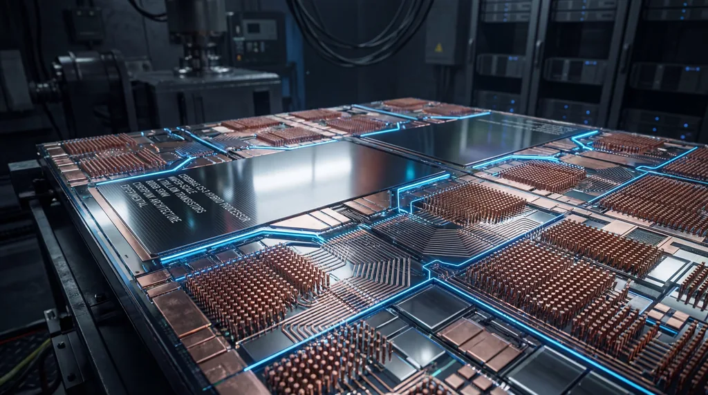
Cerebras' wafer-scale engine (WSE) is a massive system-on-wafer that integrates hundreds of thousands of AI-optimized cores and gigabytes of on-chip SRAM onto a single piece of silicon. By bypassing the traditional process of cutting wafers into small individual chips, the WSE maintains the high-bandwidth wiring inherent to the silicon manufacturing process across the entire 215mm x 215mm surface. This design allows for a mesh architecture that supports ultra-low-latency communication, which is critical for executing memory-bound operations like Large Language Model inference at scale.
The WSE functions by leveraging specialized parallelism strategies, such as MeshGEMM and MeshGEMV, to optimize distributed memory access. In a standard GPU, high-bandwidth memory (HBM) is located outside the processor, creating a bottleneck; however, the wafer-scale approach places the memory directly adjacent to the compute cores. This architecture allows the system to manage the massive data movement required for model prefilling and token generation without the power-hungry and slow process of fetching data from external components, resulting in orders-of-magnitude faster performance for AI workloads.
Wafer-Scale Integration and Hybrid Bonding Explained
Wafer-on-wafer (WoW) hybrid bonding is a cutting-edge manufacturing technique that vertically stacks two silicon wafers to create a high-density 3D interconnect. Unlike traditional packaging methods that use micro-bumps or solder to connect chips, hybrid bonding fuses the copper pads of two wafers directly together. This provides a significantly higher number of connection points per square millimeter, effectively doubling or tripling the available communication area between processing elements (PEs) and allowing for much more complex network topologies in Wafer-Scale AI systems.
- Increased Interconnect Density: Hybrid bonding allows for millions of vertical connections across the wafer surface.
- Reduced Parasitic Capacitance: The direct copper-to-copper interface lowers the electrical resistance and energy required to transmit bits.
- Enhanced Thermal Management: Stacking wafers can improve heat dissipation pathways when combined with advanced liquid cooling.
- Reticle Integration: The process allows for seamless communication between the rectangular "reticles" (the basic units of chip manufacturing) that make up the wafer.
How does physical reticle placement affect network topology in wafer-scale chips?
Physical reticle placement dictates the achievable network topology by defining the boundaries where high-speed on-chip wiring must transition into inter-reticle or inter-wafer links. In a standard Wafer-Scale AI design, the lithography process limits the size of a single functional unit (the reticle), requiring a stepping pattern to cover the entire wafer. The researchers, including Luca Benini, Torsten Hoefler, and Maciej Besta, found that the way these reticles are aligned—whether they are perfectly stacked or shifted—determines the path data must take, directly impacting latency and throughput.
Sophisticated placement strategies can significantly reduce the "hop count" between distant processing cores. The research team investigated four primary configurations: Aligned, Interleaved, Rotated, and Contoured. By strategically shifting or rotating the reticles during the hybrid bonding process, they were able to create shortcut paths that would be impossible in a standard 2D mesh. For example, a "Contoured" placement allows the network to follow the natural circular shape of the wafer, optimizing the use of edge-case silicon and creating a more efficient global communication fabric for deep learning tasks.
Optimizing Topology: The Four Reticle Placement Strategies
The baseline for wafer-scale networks is typically a 2D mesh, which is limited by its rigid, grid-like connectivity. While functional, the 2D mesh suffers from high latency when data must travel from one side of the wafer to the other. To address this, the research presented by Hoefler and his colleagues suggests that the physical arrangement of the wafers can be manipulated to create "express lanes" for data. The Aligned and Interleaved strategies focus on simplifying the vertical connections between two bonded wafers to ensure that every processing core has a direct partner on the opposite layer.
Advanced configurations like the Rotated and Contoured placements represent a breakthrough in high-performance network design. The Rotated strategy involves turning one wafer by 90 degrees before bonding, which transforms the physical layout into a high-radix network. This configuration allows for "long-range" hops across the wafer without adding extra physical wiring. These optimized topologies ensure that the network can handle the erratic data patterns often seen in sparse AI models, providing a flexible infrastructure that can adapt to different neural network architectures.
Quantifying the Gains: Performance and Efficiency
The implementation of optimized reticle placement strategies resulted in a massive 250% increase in network throughput compared to traditional 2D mesh baselines. This performance jump is primarily due to the reduction in network congestion; by providing more direct paths for data, the system can move larger volumes of information simultaneously. For Large Language Models, this means that the "all-reduce" and "all-to-all" communication patterns, which often stall training, can be completed in a fraction of the time.
Beyond raw speed, the research highlights significant improvements in latency and energy sustainability.
- Latency Reduction: Communication delays were slashed by up to 36%, enabling faster synchronization of model weights.
- Energy Efficiency: The energy required per transmitted byte decreased by up to 38%, a critical metric for the environmental impact of AI.
- System Reliability: By reducing the number of hops and the electrical distance data must travel, the researchers also improved the overall robustness of the communication fabric.
Industry Implications: From Cerebras to Future Super-Chips
This research provides a roadmap for the future of semiconductor manufacturing, moving beyond the limits of individual GPU chips. While companies like Cerebras Systems have already proven the viability of wafer-scale engines, the work of Torsten Hoefler and his team at ETH Zurich suggests that we are only at the beginning of what is possible. By utilizing wafer-on-wafer bonding and advanced topology design, future super-chips could house trillions of transistors in a single package, providing the hardware necessary to train models far larger than GPT-4.
The shift toward integrated Wafer-Scale AI will likely redefine the competition in the AI hardware market. As the demand for LLMs continues to skyrocket, the ability to minimize energy consumption while maximizing throughput will become the primary competitive advantage. The transition from building "clusters of chips" to "wafer-scale systems" represents a fundamental change in how we think about computer architecture, promising a future where the physical size of our hardware is the only limit to the intelligence of our models.

Comments
No comments yet. Be the first!