
In the rapidly evolving landscape of nanophotonics, the ability to manipulate light at the subwavelength scale has opened the door to revolutionary technologies, from ultra-thin flat lenses to advanced holographic displays. However, the engineering of these components—known as metasurfaces—has long been bottlenecked by the sheer computational complexity of their design. Traditionally, researchers have relied on grueling iterative simulations to find the precise arrangement of nanopillars required to achieve a specific electromagnetic outcome. A groundbreaking new study by Mathys Le Grand, Pascal Urard, and Denis Rideau has introduced a paradigm shift by adapting the generative principles behind high-end AI tools, such as Stable Diffusion, to automate and accelerate this process. By leveraging diffusion-based generative frameworks, the researchers have demonstrated a method to generate intricate nanostructures that meet exacting electromagnetic specifications in mere minutes, a feat that previously required hours or even days of supercomputing time.
The Complexity of Inverse Design in Nanotechnology
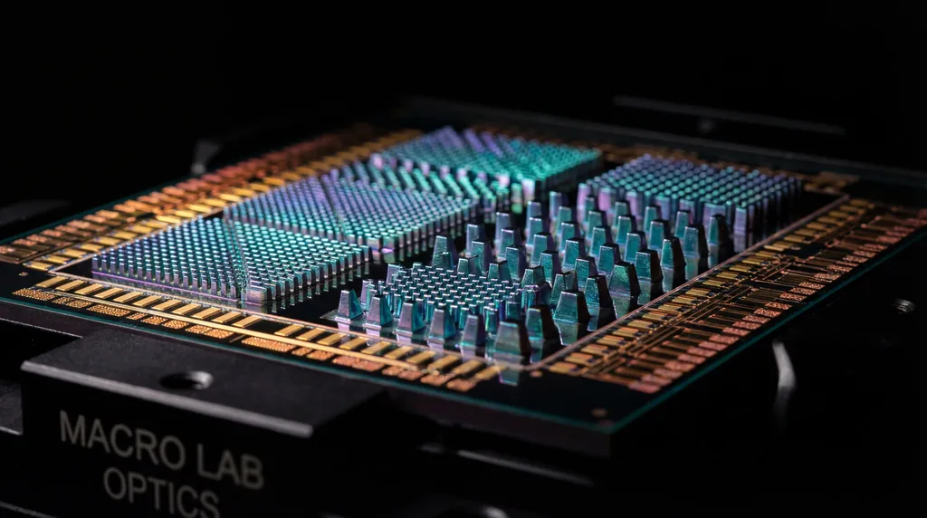
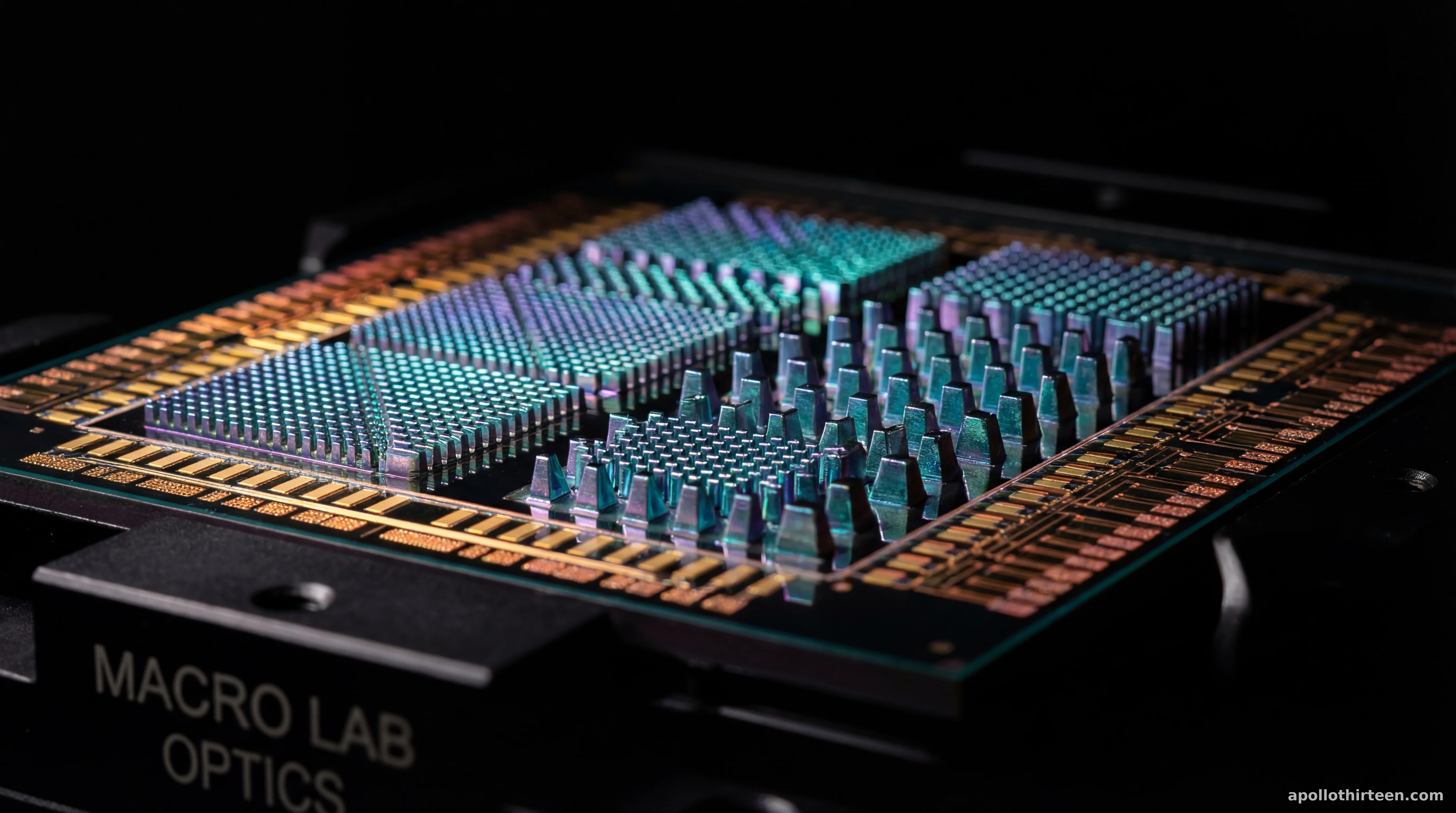
To understand the significance of this advancement, one must first grasp the "inverse design" problem inherent in nanotechnology. In conventional forward design, an engineer specifies a geometry and then calculates its physical properties. Inverse design flips this: a researcher starts with a desired optical performance—such as a specific phase shift or light-scattering pattern—and must work backward to determine the exact geometric configuration of thousands of silicon or titanium dioxide nanopillars. The relationship between a nanostructure’s geometry and its electromagnetic behavior is profoundly non-linear and multidimensional, creating a mathematical landscape that is notoriously difficult to navigate.
Current industry standards often rely on gradient-based optimization or "trial-and-error" heuristics. While effective for simple structures, these methods are prone to converging on "suboptimal solutions"—mathematical traps where the design is functional but far from the peak efficiency required for high-performance applications. Furthermore, as the scale of the metasurface grows, the computational cost of these iterations increases exponentially. This "curse of dimensionality" has historically limited the complexity of what engineers could feasibly design, often forcing a compromise between the size of the device and its optical precision.
Applying Diffusion Models to Physical Hardware
The innovation proposed by Le Grand and his colleagues involves the use of diffusion models, a class of generative AI that has recently dominated the field of computer vision. Unlike standard neural networks that might attempt to map an input directly to an output, diffusion models learn the underlying distribution of "valid" designs by systematically adding noise to a dataset and then learning the intricate process of reversing that noise to recover a clean structure. In this context, the model learns the "language" of electromagnetic metasurfaces, understanding which geometric patterns are physically viable and which are not.
However, simply generating an image of a metasurface is not enough for hardware engineering; the design must adhere to rigid physical laws. To bridge the gap between creative generation and physical accuracy, the research team integrated a dedicated consistency constraint and advanced posterior sampling methods. This ensures that every design generated by the AI is not just a visual approximation, but a mathematically sound structure capable of meeting the required electromagnetic specifications. By guiding the diffusion process toward these constraints, the framework effectively "filters" the generative output, ensuring high-fidelity results that are ready for manufacturing.
Scalability and the Leap to Large-Scale Nanostructures
One of the most striking aspects of this research is its scalability. Many AI models in the physical sciences are limited by the data they were trained on; a model trained to design small arrays often fails when tasked with larger, more complex systems. Le Grand, Urard, and Rideau addressed this by introducing a scalable methodology that allows the model to generalize its findings. After validating the framework on small-scale metasurface configurations to establish accuracy and reliability, the team extended the capability to large-scale arrays consisting of up to 98 × 98 nanopillars.
The efficiency of this approach is remarkable. The researchers demonstrated that a model trained on substantially smaller arrays—specifically 23 × 23 nanopillars—could be leveraged to generate much larger, high-precision designs. This capability effectively bypasses the need for the massive datasets that usually accompany large-scale simulations. According to the study, this framework enables the generation of designs in approximately one minute, representing a several-order-of-magnitude improvement over traditional optimization workflows that struggle with such high-density configurations.
Real-World Implications for Photonics and Beyond
The implications of this AI-accelerated design process for the field of photonics are profound. Metasurfaces are the building blocks of next-generation optical devices, including flat lenses for smartphone cameras that could eliminate the "camera bump," or lightweight augmented reality (AR) glasses that require complex light steering in a compact form factor. By reducing the design cycle from days to minutes, this research allows for a more iterative and experimental approach to hardware discovery. Engineers can now explore thousands of design permutations in the time it previously took to test one, potentially uncovering novel nanostructures that human intuition or traditional algorithms would have missed.
Beyond specific applications in holography and optical sensors, this work signals a broader shift in how we approach physical manufacturing. We are moving away from an era of laborious manual optimization toward a future of "generative engineering." In this future, the designer defines the goal, and the AI—acting as a high-speed architect—provides the optimal blueprint. The study highlights how generative AI can be more than just a tool for creating digital art; it can be a rigorous scientific instrument capable of solving some of the most complex geometry-to-physics problems in modern engineering.
Future Directions in Generative Physical Design
Looking forward, the research team suggests that this framework is only the beginning. The next step in this evolution involves the integration of manufacturing constraints directly into the generative process. While the current model ensures electromagnetic accuracy, future versions could account for the specific limitations of lithography and etching processes, ensuring that the generated designs are not only optically perfect but also easy to mass-produce. Furthermore, extending this diffusion-based approach to other domains of physics, such as acoustics or thermal management, could lead to similar breakthroughs in those fields.
The work of Mathys Le Grand, Pascal Urard, and Denis Rideau provides a robust foundation for a new era of high-precision inverse design. By combining the probabilistic power of diffusion models with the rigid requirements of electromagnetic theory, they have created a tool that bridges the gap between artificial intelligence and physical reality. As these models become more sophisticated, the boundary between what we can imagine and what we can build at the nanoscale will continue to blur, driven by the silent, rapid calculations of generative AI.

Comments
No comments yet. Be the first!